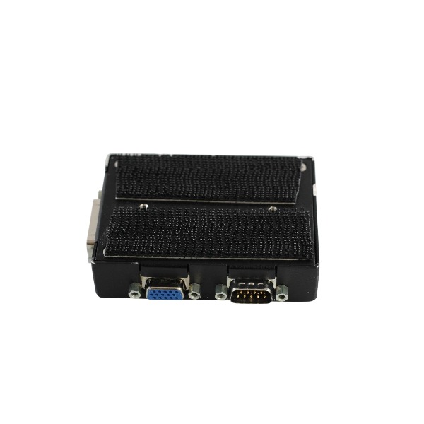












Description
-
BrandAMAT
-
Model0010-23715
-
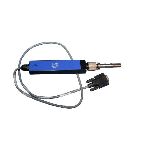
Product NamePMAX Emissometer Sensor Probe
-
Place of OriginUnited States
-
Customs HS Code84869000
-
Power Supply0.10A
-
Dimensions120mm × 32mm × 28mm
-
Weight0.21kg
-
Operating Temperature10°C to +50°C
-
Storage Temperature-20°C to +60°C
-
Warranty12 month
-
Product Statusnew
AMAT 0010-23715 PMAX Pyrometer / Emissometer Probe Assembly Features
Product type: PMAX optical pyrometer and emissometer probe assembly
Application: Developed to measure wafer temperature and emissivity for AMAT Centura and Endura semiconductor process platforms
Optical design: Integrated infrared optical path enabling non-contact thermal measurement of wafers
Connector: 25-pin high-density D-Sub interface
Power requirement: Regulated 10–50 VDC power supply
Signal output: Differential analog signals for temperature and emissivity feedback
Communication: Serial diagnostic port supporting AMAT proprietary protocol and SECS/GEM host communication
Housing: Metallic vacuum feedthrough structure suitable for chamber vacuum conditions
Sealing: Built-in O-ring to provide vacuum sealing at the bulkhead mounting port
Purge interface: Optical purge gas port to mitigate process film accumulation on the optical window
Anti-interference: Requires shielded twisted-pair cabling with single-point shield grounding to suppress ground loops and plasma electromagnetic interference
Protection: Electrostatic-sensitive device; handling must follow ESD control procedures
Measurement function: Real-time wafer temperature and emissivity monitoring to support thin-film process control
Compatibility: Works in conjunction with the AMAT PMAX controller system

AMAT 0010-23715 PMAX Pyrometer / Emissometer Probe Assembly Application Cases
Case 1: Rapid Thermal Processing (RTP) Annealing – Centura Platform
This probe is mounted on the bulkhead of AMAT Centura RTP chambers for front-end wafer annealing processes. It performs non-contact, real-time measurement of wafer temperature and surface emissivity during source/drain doping spike annealing. The device compensates emissivity fluctuations induced by polysilicon and silicide thin films, stabilizes peak temperature control accuracy, and minimizes transistor threshold voltage deviation. All process data is transmitted to the host system via SECS/GEM protocol to achieve full lot traceability.
Case 2: Dielectric Film Deposition – Endura Platform
Implemented in Endura PECVD chambers for high-k gate dielectric and silicon oxide film deposition. The probe continuously monitors wafer thermal conditions under high-temperature deposition environments. It feeds precise differential analog thermal signals back to the PMAX controller for dynamic lamp power adjustment, effectively improving within-wafer film thickness uniformity and reducing process particle generation and product defect rates.
Case 3: Metal Barrier & Seed Layer PVD Process
Applied in Endura PVD chambers for the deposition of TiN/TaN barrier layers and copper seed layers used in chip interconnect structures. Plasma environment changes and stacked thin-film structures cause continuous emissivity variation. The probe delivers real-time emissivity calibration to correct pyrometer measurement data, preventing wafer overheating or insufficient heating, and ensuring consistent and stable contact resistance of copper via structures.
Case 4: High-Temperature Oxidation & Diffusion Process
Utilized in thermal oxidation and post-ion-implantation diffusion process chambers. It accurately tracks wafer temperature throughout long-cycle, high-temperature oxidation procedures. Equipped with an optical purge interface, the probe effectively prevents oxide deposition contamination on the optical lens, sustaining long-term measurement stability and reducing chamber preventive maintenance frequency.
Case 5: Semiconductor Process R&D and Recipe Qualification
Deployed on laboratory-grade Centura R&D equipment for new process recipe development and verification, covering low-power logic chips and memory device process validation. It provides high-precision thermal measurement data for recipe optimization, supports data comparison under diverse thin-film stack structures, and enables reliable qualification of new process materials prior to mass production deployment.
Case 6: Advanced 3D Packaging TSV Thermal Process
Adopted for thermal annealing and reflow processes of through-silicon vias (TSV) in 3D heterogeneous packaging. The probe captures transient wafer temperature changes during thermal cycling, effectively avoiding TSV delamination and thermal stress-induced defects, and satisfies the stringent thermal budget control requirements of advanced semiconductor packaging integration.



.jpg)